The Need for Speed
Deep learning has emerged as the most important computational workload of our generation. Tasks that historically were the sole domain of humans are now routinely performed by computers at human or superhuman levels.
Deep learning is also profoundly computationally intensive. A recent report by OpenAI showed that, between 2012 and 2018, the compute used to train the largest models increased by 300,000X. In other words, AI computing is growing 25,000X faster than Moore’s law at its peak.
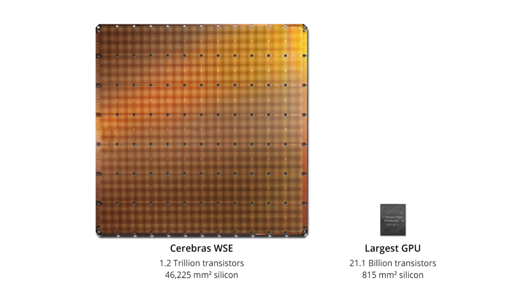
To meet the growing computational requirements of AI, Cerebras has designed and manufactured the largest neural network chip ever built. The Cerebras Wafer Scale Engine (WSE) is 46,225 millimeters square, contains more than 1.2 trillion transistors, and is entirely optimized for deep learning workloads.

By way of comparison, the WSE is more than 56X larger than the largest graphics processing unit (GPU), containing 3,000X more on chip memory and more than 10,000X the memory bandwidth.
But Why Do We Need a Big Chip? Why Not Just Tie Together Lots of Smaller Chips?
At Cerebras, we began with a clean sheet of paper and a desire to build a new type of computer that is optimized exclusively for deep learning. Choosing the right computer architecture for a specific workload is like finding the right design for a car. The first question to ask is: What is its job? Will it be taking children to soccer practice? Or will it be moving bricks and lumber? These questions determine whether a minivan or a pickup truck is the right solution. In computer design, too, understanding the computer’s workload — in this case neural network processing — is the first step.
The Deep Learning Workload
An artificial neural network used as a model in deep learning is a sequence of data transformations, or layers, arranged from the input (where data flow in) to the output (where, for example, classification predictions or translated sentences or “Go” moves flow out). The transformation at each layer is parameterized by the model parameters of that layer and dominated by a simple, highly parallel operation, such as multiplying a vector (the input data) by a matrix (the model parameters).
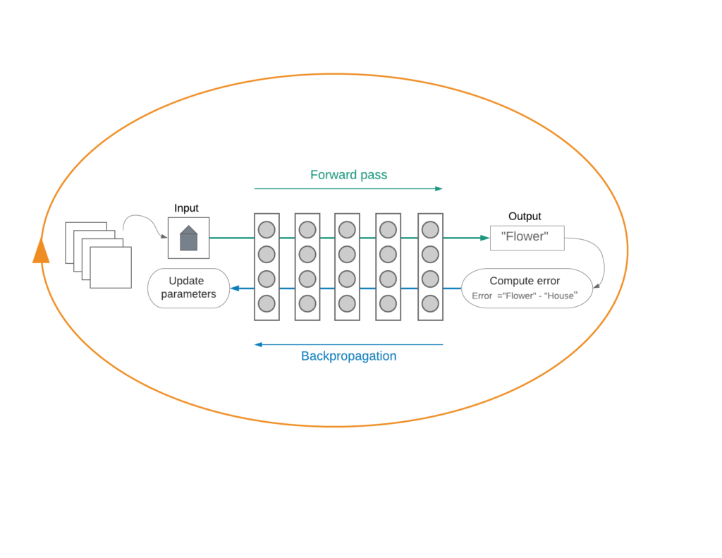
During model training, labeled data samples flow from input to output (I to O) through all layers of parametrized transformations — a forward pass. At the output end, the output, or prediction, is compared to the correct answer for that particular input. Prediction error is computed; error being the difference between the predicted output and the correct one. Then, the error begins to work its way backwards in the O-to-I direction, via the backpropagation algorithm. As the error flows through each layer, it interacts with the I-to-O data that produced it (that data has been parked there, waiting for the error to come back) and, together, they determine how to change the layer’s parameters to most effectively reduce the error. The parameters are then adjusted, and this process of forward-backpropagation steps continues for numerous passes over the set of training examples, until the error becomes insignificant or doesn’t decrease anymore. Essentially, a multi-stage training loop is created.
Understanding Performance
Thinking about a deep neural network (DNN) as a multistage computational feedback loop helps us understand its performance characteristics, and the architectural choices made by startups and incumbents alike.
To reduce training times, one must reduce the time it takes for inputs to travel through the calculation and communication components of the feedback loop. So, calculations and communication must be accelerated. Accelerating calculation is most directly achieved by increasing the number of compute cores. More cores — specifically more floating point multiply accumulate units (FMACs) — do more calculations in less time. Placing high-speed memory close to cores ensures that the cores are constantly fed with data to perform calculations. Placing memory far away, off-chip means the cores are frequently idling, and not performing useful computations.
High-bandwidth, low-latency communication among the compute cores ensures that the cores can be gathered together into groups to quickly solve problems that would take a single core too long to do. In addition, high-bandwidth, low-latency communication ensures that the results of each stage in the loop are delivered fast to the subsequent stages waiting on them.
With this simplistic understanding of deep learning performance knobs, we understand the competitive landscape in AI compute.
The fewer big cores in CPUs weren’t designed for the type of calculations in a multistage training loop. The more numerous little cores in GPUs weren’t designed for AI work either, but there were more of them, and that carried the day. This logic also explains why, over the past six years, Nvidia’s GPUs have grown from 551 square millimeters to 815 square millimeters. More silicon area provides more room for cores and more cores deliver more calculations. More silicon area also provides more room for memory close to cores. Thus, for training, GPUs have dominated CPUs recently.

These insights also explain the recent focus on communication fabrics. As AI compute became more demanding, the number of cores needed in the training loop exceeded the number of cores on a single neural network chip. Having reached the traditional limit to neural network chip size, the only way to get more cores was to string more chips together into clusters. However, off-chip communication is tens of thousands of times slower than on chip communication. Linking together cores from different chips to work on a single problem became a vital problem, and informs why NVIDIA designed NVLink to improve communication among chips, and their acquisition of Mellanox for $6.8B — Mellanox pioneered InfiniBand, a communication technology for linking chips together.
This same logic helps to contextualize the claims made by many startups in the AI acceleration space. Some claim that they have moved more memory onto the chip to increase the efficiency of core calculations. Others claim they more tightly tune their cores for AI work to get more calculations per unit time, or to avoid doing useless work like multiplying by zero.
Fundamentally, all of these strategies are trying to drive up calculation and accelerate communication through one or more of three strategies: 1) more/better cores, 2) more memory close to cores, and 3) more low-latency bandwidth between cores.
But What Would Happen if You Took These Three Approaches to Their Logical Extreme?
You would get a very big neural network chip, with memory close to cores, all connected by a high-bandwidth, low-latency fabric.
How might this be achieved? Small neural network chips are built as arrays of identical chips on a 12-inch diameter silicon wafer. To get a really big chip, instead of cutting the wafer into small chips, you would increase the size of the chip to a full wafer. That would dramatically increase the number of cores available to do calculations. Now that you had sufficient silicon area, you would distribute memory across the chip, giving each core its own local memory.
Finally, you would build a communication fabric across all the cores since the communication would all be on-die, where it is many thousands of times faster than off-chip technologies like PCIe, NVLink or InfiniBand, simply due to the laws of physics.
So, why hasn’t this been done before? Because it is very difficult. Nobody has ever built and brought to market a chip larger than 840 mm². The design, manufacturing, power, cooling, communication and coordination challenges are immense. But the promise is huge. The resulting chip would be 50x larger than the largest chip on the market today. It would have hundreds of thousands of AI optimized cores and Gigabytes of on-chip memory distributed across the cores. And it would have petabytes/s of core-to-core bandwidth.
The Cerebras Architecture: Accelerating Deep Learning
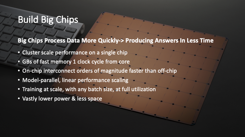
The Cerebras Wafer Scale Engine is dedicated to accelerating both deep learning calculation and communication, and by so doing, is entirely optimized for reducing training time. The approach is a straightforward function of the size of the WSE. By building a wafer-scale chip and keeping everything on a single piece of silicon, we can avoid all the performance pitfalls of slow off-chip communication, distant memory, low memory bandwidth, and wasting computational resources on useless work. We can deliver more cores optimized for deep learning primitives; more local memory close to cores for efficient operation; and more high-performance, low-latency bandwidth between cores than can be achieved by off-chip interconnects. In other words, the WSE achieves cluster-scale performance on a single chip, without the penalties of building large clusters and the limitations of distributed training.
More Silicon Area Means More Space for Compute Cores
The Cerebras Wafer Scale Engine delivers 400,000 programmable compute cores, called Sparse Linear Algebra Cores, or SLA™ cores. They are optimized for the mathematical operations that are fundamental to neural networks. These cores are small and fast, contain no caches, and have eliminated other features and overheads that are needed in general-purpose cores.
SLA cores are programmable, ensuring that they can run all neural network algorithms in the constantly changing field of deep learning. Each core performs both control processing and data processing. Control processing, used for parallel processing coordination, is achieved with a full set of general-purpose instructions, which provide programmable primitives such as arithmetic, logical, and branching operations. They provide the foundation on which any parallel algorithm can be mapped. The data processing is for the math at the heart of neural networks.
Tensor operations are at the core of the neural network workload. To achieve high performance, the SLA cores have a specialized tensor processing engine where full tensors are first-class operands. Programmability ensures that the same engine can be used to perform a variety of tensor operations such as convolution or matrix multiply. The hardware internally optimizes the tensor processing to achieve datapath utilization three of four times greater than GPUs.
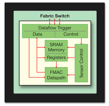
To deal with sparsity that is abundant in neural network workloads, Cerebras invented sparsity harvesting technology, which allows the SLA cores to intelligently skip the zeros that are often prevalent in neural network workloads.
Multiplying by zero is a waste — a waste of silicon, power, and time, all while creating no new information. Due to key deep learning functions such as the rectified linear unit nonlinearity (ReLU) and dropout, zeros are introduced into neural network tensors. Newer methods are emerging around weight sparsity that add even more zeros. Put simply, there is a growing interest in making tensors sparser still.
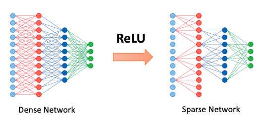
GPUs and tensor processing units (TPUs) are dense execution engines; they perform the same computation task on an entire vector or matrix of data. This is a wise approach when the vector or matrix is dense (all nonzero). In the dense environment, efficiencies are gained by bunching the data together and providing a single instruction to be applied to all of the data — an approach called SIMD. But when the data is 50 to 98% zeros, as it often is in neural networks, then 50 to 98% of multiplications are wasted.
The Cerebras SLA core never multiplies by zero. It has built-in, fine-grained dataflow scheduling, so compute is triggered by data arrival. The scheduling operates at the granularity of a single data value so only non-zero data triggers compute; all zeros are filtered out. In other words, the SLA core never multiplies by zero nor does it propagate zeros across the fabric. This in turn provides a performance advantage by doing useful work during those cycles, which otherwise would be wasted, not to mention power and energy savings.
The computer architect’s mantra — optimize for the most useful work — is brought to the forefront with sparsity. And with the WSE, we have made sure that all 400,000 AI-optimized cores never multiply by zero, providing an architectural foundation for extraordinary performance.
More Silicon Area Means More on-Chip Memory
Memory is another key component of any computer architecture. More memory close to cores means faster calculations, lower latencies, and less power consumed in moving data. High-performance deep learning requires each core to operate at maximum utilization, which requires close collaboration and proximity between the core and memory.
In deep learning, memory is used to hold a model’s parameters, activations, configuration data, and more. In state-of-the-art-networks, model parameters run into the gigabytes, with this memory requirement expected to grow.
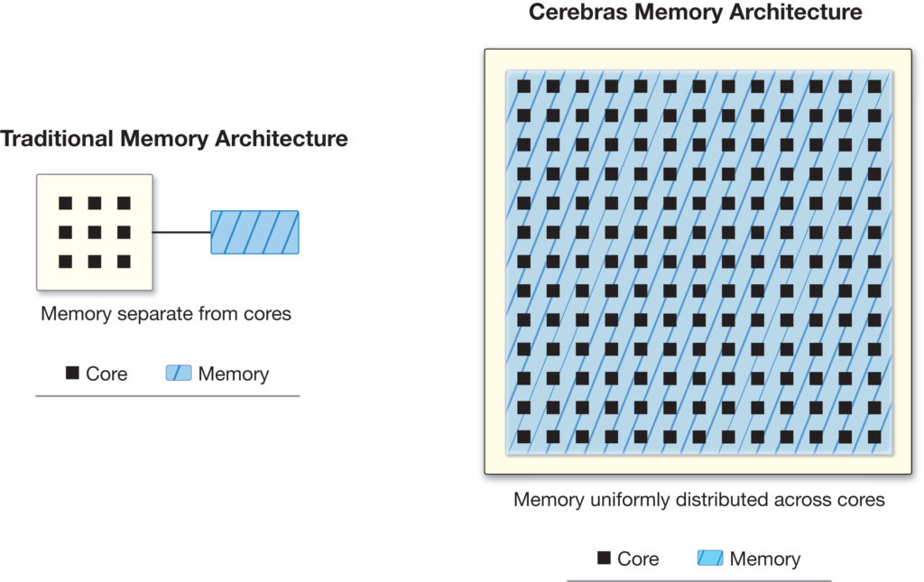
For maximum performance, ideally the entire model would fit in the fastest memory, closest to the computation cores. This is not the case in traditional chip architectures, where main memory is not integrated with compute. Instead, the vast majority of memory is off-chip, far away on separate DRAM chips or a stack of high bandwidth memory (HBM). As a result, main memory is excruciatingly slow.
While computer architects have tried for decades to address the memory bottleneck, the primary solution has been memory hierarchies — many levels of on-chip and near-chip caches. These are costly, small, and provide sometimes unpredictable benefits. Once the on-chip/off-chip boundary is crossed, the latency-to-memory explodes and bandwidth plummets. It forces a downward spiral of performance, and is one of the fundamental reasons GPUs are challenged when doing artificial intelligence work.
Cerebras has solved this problem. The WSE has 18 Gigabytes of on chip memory and 9.6 Petabytes of memory bandwidth — respectively, 3,000x and 10,000x more than is available on the leading GPU. As a result, the WSE can keep the entire neural network parameters on the same silicon as the compute cores, where they can be accessed at full speed. This is possible because memory on the WSE is uniformly distributed alongside the computational elements, allowing the system to achieve extremely high memory bandwidth at single-cycle latency, with all model parameters in on-chip memory, all of the time.
The Cerebras WSE delivers more compute cores, more local memory, and more memory bandwidth than any neural network chip in history. This enables fast computation, reduces the time it takes to train a model, and uses less energy as well.
More Silicon Area Enables Blisteringly Fast Communication — Swarm™ Fabric
Deep Learning is a very communication-intensive workload — layers, and therefore cores, communicate constantly — so the fabric that links cores together is fundamental to performance. Peak performance is achieved when cores can communicate at high bandwidth and low latency, since the cores can be clustered together to do in a group what would take an individual core too long to do.
A fundamental truth in computer architecture is that off-chip communication is tens of thousands of times slower than on-chip communication. Small neural network chips that wish to communicate must be clustered together via Ethernet, InfiniBand, PCIe, or other off-chip technologies, which all suffer an enormous performance penalty compared to staying on-silicon. In addition to being faster, on-chip consumes less than a thousandth the power per bit moved.
The Cerebras Swarm communication fabric creates a massive on-chip network that delivers breakthrough bandwidth and low latency, at a fraction of the power draw of traditional communication techniques used to cluster GPUs together.
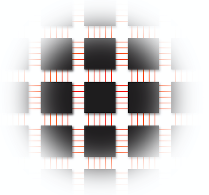
The 400,000 cores are connected via the Swarm in a 2D mesh with 100 Petabits per second of bandwidth. Swarm provides a hardware routing engine to each of the compute cores and connects them with short wires optimized for latency and bandwidth. The resulting fabric supports single-word active messages that can be handled by the receiving cores without any software overhead. It is also fully configurable; software configures all cores on the WSE to support the precise communication required for training the user-specified model. Thus for each neural network, Swarm provides a unique and optimized communication path. On CPUs and GPUs, all neural networks are shoehorned into one hard-coded on-chip communication path.
Typical Swarm messages traverse a link with nanosecond latency. Communication software such as TCP/IP and MPI is not needed, avoiding associated performance penalties. The energy cost of communication in this architecture is well below one picojoule per bit, nearly two orders of magnitude lower than CPUs or GPUs. As a result, the WSE trains models faster and uses less power.
Conclusion: WSE, The Future of AI Computation
The Cerebras WSE is the largest chip ever built. It is 46,225 square millimeters and contains 1.2 Trillion transistors and 400,000 AI-optimized compute cores. The memory architecture ensures each of these cores operates at maximum efficiency. It provides 18 gigabytes of fast, on-chip memory distributed among the cores in a single-level memory hierarchy one clock cycle away from each core. These high-performance, AI-optimized, local memory-fed cores are linked by the Swarm fabric, a fine-grained, all-hardware, high bandwidth, low latency mesh-connected fabric.
By accelerating deep learning compute, the WSE eliminates the primary impediment to the advancement of artificial intelligence by reducing the time it takes to train models from months to minutes and from weeks to seconds. It enables deep learning practitioners to test hypotheses more quickly and to explore ideas that today are untestable with legacy architectures or are too expensive to try. The WSE reduces the cost of curiosity, accelerating the arrival of the new ideas and techniques that will usher forth tomorrow’s AI.
Take a look at the CS-1 product overview for more details about the Wafer Scale Engine — the largest neural network chip.
Related Posts
May 17, 2024
Cerebras Breaks Exascale Record for Molecular Dynamics Simulations
Cerebras has set a new record for molecular dynamics simulation speed that goes…
May 1, 2024
Supercharge your HPC Research with the Cerebras SDK
Cerebras SDK 1.1.0, our second publicly available release, includes initial…
1 Comment
Add comment Cancel reply
You must be logged in to post a comment.




[…] Chips, Challenges and Market Trends: Interesting trend observed recently when Cerebras rolled out biggest chip called wafer scale engine with 1.2 trillion transistors justifying the need for biggest chip for deep learning. More details on this is https://cerebras.net/blog/cerebras-wafer-scale-engine-why-we-need-big-chips-for-deep-learning/ […]